
Product usage display
Wide range of applications suitable for a variety of products
CY-XB01-150 wave-absorbing material is used for FC, RFID, high-frequency electronic components of motherboards, communication products, GPS, laptops, TVs, audio, computers, digital cameras, game consoles, microwave ovens, smart payment mobile phones, POS machine, various smart cards, RFID radio frequency cards, RFID reader/writer, various smart access control, WIF, etc.

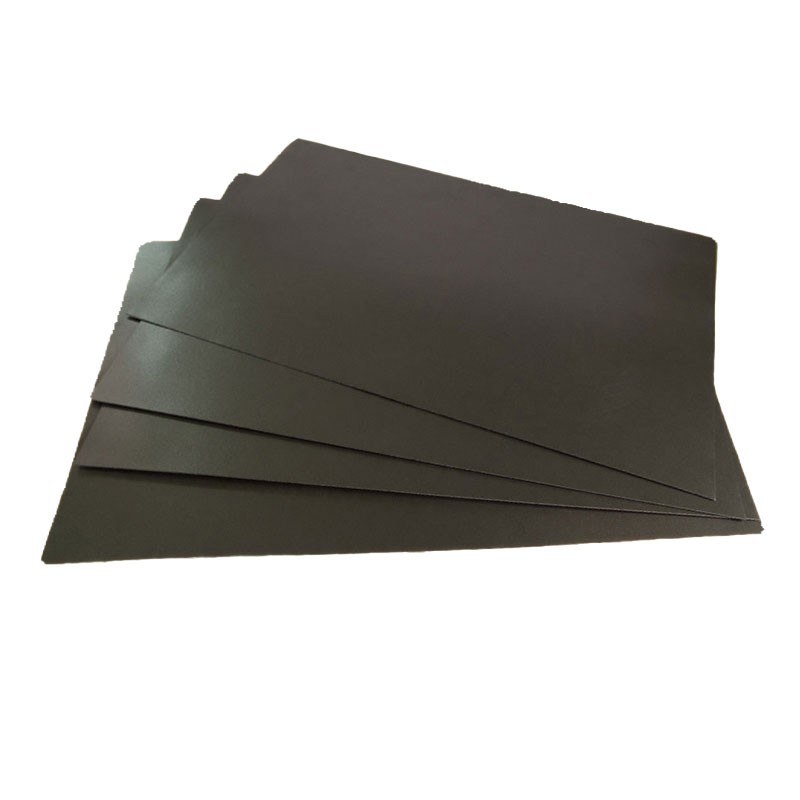
Name: Absorbing material
Process: Conventional adhesive PET double-sided tape (thickness: 0.05mm), other adhesives can be customized according to customer requirements, and various special-shaped specifications can also be customized according to customer drawings)
Function: Reduce electromagnetic wave interference
Magnetic permeability: 50U, 110U, 120U, 150U (±10%)
Performance: light weight, temperature-resistant, moisture-resistant, and corrosion-resistant. The reading distance attached to metal is farther than that without metal attachment. This is the excellent result of the overall design.
Principle: It mainly relies on the medium that is isolated from the metal, and uses the metal as a reflective surface to improve the characteristics of the label on the metal.
Physical properties:
1. anti-metal tags are electronic tags encapsulated with a special anti-magnetic wave-absorbing material, which technically solves the problem that electronic tags cannot be attached to metal surfaces.
2. The product is waterproof, acid-proof, alkali-proof, and collision-proof, and can be used outdoors.
Features:
1. Pasting anti-metal electronic tags on metal can achieve good reading performance, and can even read farther than in the air.
2. Using special absorbing materials, this type of material can effectively prevent metal from interfering with radio frequency signals.
Detailed explanation;
1. In RFID equipment, electronic tags must be integrated or attached to the product. Due to limited space in the equipment, electronic tags are affixed to the surface of conductive objects such as metal or to places with metal devices nearby.
2. The alternating electromagnetic field induced by the tag under the action of the signal emitted by the card reader is easily affected by the eddy current attenuation of the metal, which greatly weakens the signal strength, causing the reading process to fail.
3. Therefore, it is necessary to add anti-metal absorbing materials to the product to take advantage of the property of electromagnetic waves in the medium to be conducted by low magnetic guidance and high magnetic permeability to provide a magnetic path for the electromagnetic field, enhance the magnetic induction intensity, and prevent the skin effect between electromagnetic waves and metal, thereby Improve reading distance and sensitivity.
Absorbing material:
1. The so-called absorbing material refers to a type of material that can absorb or significantly weaken the electromagnetic wave energy received on its surface, thereby reducing the interference of electromagnetic waves.
2. In Engineering applications, in addition to requiring the absorbing material to have a high absorption rate of electromagnetic waves in a wide frequency band, it is also required to have light weight, temperature resistance, moisture resistance, corrosion resistance and other properties.
introduce:
1. With the development of modern science and technology, the impact of electromagnetic wave radiation on the environment is increasing day by day.
At airports, flights are unable to take off due to electromagnetic wave interference and are delayed; at Hospitals, mobile phones often interfere with the normal operation of various electronic diagnostic and treatment instruments.
Therefore, controlling electromagnetic pollution and finding a material that can withstand and weaken electromagnetic radiation - absorbing materials - has become a major topic in materials science.
2. Electromagnetic radiation causes direct and indirect harm to the human body through thermal effects, non-thermal effects, and cumulative effects.
Research has confirmed that the performance of absorbing materials is better. It has the characteristics of high absorption frequency band, high absorption rate, and thin matching thickness.
Applying this material to electronic equipment can absorb leaked electromagnetic radiation and eliminate electromagnetic interference.
According to the law that electromagnetic waves propagate in the medium from low magnetic to high magnetic permeability, high magnetic permeability is used to guide electromagnetic waves. Through resonance, a large amount of electromagnetic wave radiation energy is absorbed, and then the electromagnetic wave energy is converted into thermal energy through coupling.
3. When designing absorbing materials, two issues should be considered:
When electromagnetic waves encounter the surface of absorbing materials, they should pass through the surface as completely as possible to reduce reflection;
When electromagnetic waves enter the interior of the absorbing material, the energy of the electromagnetic waves should be lost as much as possible;
Product Features:
For a specific frequency, the electromagnetic waves projected onto the surface of the wave-absorbing and magnetically conductive material are gathered and absorbed, and the electromagnetic wave energy is converted or consumed.
It is used in fields such as electromagnetic compatibility (EMC) and electromagnetic interference suppression (EMI) in the electronics manufacturing industry to suppress the adverse effects of electromagnetic noise on electronic equipment; or it is used in fields such as wireless charging and radio frequency signal communication to conduct electromagnetic wave energy.
Electromagnetic noise suppression: used to solve electromagnetic compatibility problems caused by electromagnetic noise, reduce coupling between electromagnetic noise paths, suppress electromagnetic noise current, reduce radiation, and effectively reduce the harm caused by electromagnetic noise interference.
>Mounted in a shielding box to absorb the electromagnetic wave reflection of the shielding box and reduce interference to electronic components;
>Mounted between PCB circuit boards or components, using wave-absorbing and magnetically conductive materials to construct magnetic paths to reduce electromagnetic field coupling;
>Mounted on LS1, IC chips or circuit board high-frequency current lines to suppress high-frequency electromagnetic radiation;
>Mounted on the flexible circuit board FPC to suppress the conduction radiation of the cable.
Contact: Adam
Phone: +86 18205991243
E-mail: sale1@rfid-life.com
Add: No.987,Innovation Park,Huli District,Xiamen,China
 Adam
Adam